A GPU is the flexible, general-purpose AI chip that trains and runs almost any model on any framework. A TPU is Google’s custom chip for large-scale tensor math, cheaper than a GPU at scale but only on Google Cloud. An NPU is a tiny, ultra-efficient chip built into phones and laptops that runs trained models on-device at a few watts. The rule of thumb: train on a GPU, scale cloud workloads on a TPU, and run inference on the device with an NPU.
Choosing between a GPU, a TPU and an NPU is now the first hardware decision in almost every AI project. Get it wrong and you either overpay by an order of magnitude or run a workload on silicon that was never designed for it.
The reason three separate chip families exist comes down to one fact: the ordinary CPU that runs everything else in computing is badly suited to the matrix mathematics behind neural networks. If you are new to the software side, our guide to AI vs machine learning sets the scene. Three specialised processors grew up to fill the hardware gap, and each took a different path.
The GPU is the all-rounder, running training and inference across every major framework. The TPU is Google’s purpose-built chip for machine learning at cloud scale. The NPU is the compact inference engine sitting in your phone, laptop and car, drawing a few watts where a data-centre GPU burns hundreds. This guide explains how each one works, where it wins, and how to match the right chip to your workload.
The AI Hardware Landscape in 2026
For decades one chip handled everything. AI changed that for good. The core operations of a neural network — matrix multiplication, tensor operations and convolutions across billions of parameters — are so unlike the sequential logic a CPU was built for that purpose-built silicon became essential, not just nice to have.
By 2026, more than 75% of AI models run on specialised accelerators rather than general-purpose CPUs. The question is no longer whether to use dedicated AI hardware. It is which type, at which layer of the stack, for which workload.
- The global AI hardware market reached $65.35 billion in 2026, on track for $296.3 billion by 2034 at an 18% CAGR.
- NVIDIA holds roughly 87% of the AI GPU market, with $51.2 billion in data-centre revenue in a single quarter (Q3 FY2026, up 66% year on year).
- NPUs now ship in over 970 million smartphones, making them the most widely deployed AI chip by unit volume.
- Custom ASIC shipments (Google TPU, AWS Trainium, Microsoft Maia, Meta MTIA) are growing 44.6% in 2026, nearly three times faster than GPU shipments at 16.1%.
Three chips, three philosophies. The sections below take each one in turn, then bring them together in a full comparison.
GPU: The General-Purpose Workhorse
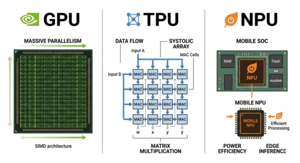
A Graphics Processing Unit is a massively parallel processor first built to render pixels, then repurposed and eventually redesigned as the default AI accelerator. A modern data-centre GPU has little in common with its gaming roots. It is a compute engine tuned for the floating-point matrix operations that power every neural network.
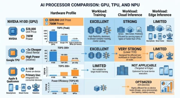
NVIDIA’s H100, built on the Hopper architecture, packs 16,896 CUDA cores, 80GB of HBM3 memory, 3,350 GB/s of memory bandwidth and up to 3,958 TOPS of INT8 performance. The Blackwell B200 pushes that to 192GB of HBM3e and over 1,000 PFLOPS of low-precision inference. What really sets GPUs apart, though, is CUDA: more than 20 years of libraries, 4 million-plus developers, and every major framework optimised for it first.
Strengths
- Universal framework support — PyTorch, TensorFlow, JAX and ONNX all target CUDA first.
- Trains anything — transformers, CNNs, diffusion models, GNNs and reinforcement learning, with no redesign.
- High memory capacity — 80GB on the H100, up to 288GB on the AMD MI350X, enough for large models without partitioning.
- Available everywhere — every major cloud offers GPU instances, and you can buy them on-premises.
Limitations
- Power-hungry — the H100 draws up to 700W; an 8-GPU server needs around 6.4kW plus cooling.
- Expensive — roughly $28,000 per H100 and $40,000-plus per B200, before a cluster trains a single model.
- Supply-constrained — TSMC CoWoS packaging limits availability, so lead times are long.
- CUDA lock-in — the same ecosystem that makes GPUs safe also makes porting to ROCm costly.
| Parameter | NVIDIA H100 / B200 (2026) |
|---|---|
| CUDA cores | 16,896 (H100) |
| Memory | 80GB HBM3 (H100) / 192GB HBM3e (B200) |
| Memory bandwidth | 3,350 GB/s (H100) |
| Performance | 3,958 TOPS INT8 (H100); 1,000+ PFLOPS FP4 (B200) |
| Power (TDP) | 700W (H100); 1,000W (B200) |
| Price | ~$28,000 (H100); $40,000+ (B200) |
| Software | CUDA, cuDNN, cuBLAS, TensorRT; PyTorch, TensorFlow, JAX |
| Interconnect | NVLink/NVSwitch; InfiniBand for cluster-scale training |
TPU: Google’s Tensor Math Engine
A Tensor Processing Unit is a custom ASIC that Google designed specifically for the matrix and tensor operations at the heart of machine learning. First deployed internally in 2015 and now in its seventh generation with Ironwood (November 2025), the TPU is built around a systolic array: a grid of multiply-accumulate units that data flows through in a wave, removing the memory bottleneck that limits GPUs on certain workloads.
The numbers are striking. Google’s first TPU delivered 83 times better performance-per-watt than contemporary CPUs and 29 times better than GPUs for inference. At scale, TPUs cost roughly half as much as equivalent GPU compute on Google Cloud, and some teams report 50% savings on matched workloads. TPUs also scale to pods of up to 9,216 chips on a proprietary interconnect.
The catch is the ecosystem. TPUs live only on Google Cloud, work best with TensorFlow and JAX, and treat PyTorch as a second-class citizen through an XLA bridge.
Strengths
- Cost-efficient at scale — about 2x cheaper than GPU for matched large workloads.
- Massive pod scaling — up to 9,216 chips on one interconnect, with far less cluster engineering.
- Energy-efficient — strong perf-per-watt on large-batch ML at data-centre scale.
- Battle-tested — powers Google Search, Photos, Translate and its largest language models.
Limitations
- Google Cloud only — no multi-cloud, no on-premises deployment.
- Framework dependency — tuned for TensorFlow and JAX; PyTorch support trails.
- Workload-specific — great for large batch matrix math, weaker on irregular or dynamic shapes.
- Harder to debug — fewer tools and a smaller community than CUDA.
| Parameter | Google TPU Ironwood v7 (2026) |
|---|---|
| Architecture | Systolic array of multiply-accumulate units |
| Scale | Up to 9,216 TPUs per pod; chips, slices and full pods |
| Performance | Hundreds to thousands of TOPS, varies by configuration |
| Memory | HBM2e per chip; pod memory scales to petabytes |
| Availability | Google Cloud only; Vertex AI integration |
| Frameworks | TensorFlow, JAX native; PyTorch via XLA |
| Cost | ~2x cheaper than GPU at scale for matched workloads |
NPU: The Edge Inference Specialist
A Neural Processing Unit is a small, ultra-low-power accelerator built to run trained models on edge devices: phones, laptops, tablets, cars, sensors and industrial equipment. These are places where cloud connectivity may be missing, latency must be measured in milliseconds, power budgets are watts rather than kilowatts, and privacy demands that data stay local.
Unlike GPUs and TPUs, NPUs do one job: inference. They run an already-trained model against new input as fast and efficiently as possible. By dropping general programmability in favour of fixed-function neural circuits, they reach 40 to 60 times the energy efficiency of GPUs for edge inference.
Apple’s Neural Engine in the M4 delivers 38 TOPS within about a 25W chip budget. Qualcomm’s Hexagon NPU in the Snapdragon X Elite delivers 45 TOPS. Intel’s Core Ultra NPU delivers 13 TOPS. With over 970 million NPU-equipped smartphones shipped in 2025, the NPU is the most widely deployed AI chip on the planet, even though most people have never heard the name.
Strengths
- Extreme efficiency — 40 to 60x more power-efficient than a GPU for inference.
- Zero cloud cost — once deployed, on-device inference has no per-query charge.
- Privacy-first — data never leaves the device, ideal for health and biometrics.
- Ultra-low latency — under 10ms on-device versus 100 to 500ms for a cloud round-trip.
Limitations
- Inference only — NPUs cannot train models.
- Model size limits — roughly 1 to 7 billion parameters on-device in 2026.
- Optimisation required — models must be quantised and compiled with vendor toolchains.
- Vendor fragmentation — Apple, Qualcomm, MediaTek, Samsung, Intel and Arm each differ.
| Parameter | 2026 Flagship NPUs |
|---|---|
| Apple M4 Neural Engine | 38 TOPS; Core ML toolchain |
| Qualcomm Hexagon (Snapdragon X Elite) | 45 TOPS; SNPE toolchain |
| Intel AI Boost (Core Ultra) | 13 TOPS; OpenVINO toolchain |
| Power | 4 to 10W typical, 40 to 60x more efficient than a GPU for inference |
| Model support | Up to 1 to 7B parameters; MobileNet, EfficientNet, small LLMs |
| Deployment | Core ML, SNPE, OpenVINO, ONNX Runtime, TensorFlow Lite |
Architecture Deep Dive
Matrix multiplication is the operation that happens billions of times a second inside a neural network. The three chips differ most in how their silicon carries it out.
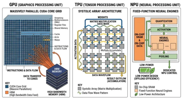
GPU approach
Thousands of flexible cores run independently, scheduling matrix work dynamically. Tensor Cores accelerate mixed-precision math.
High-bandwidth memory feeds the cores. Flexibility runs any model, but spends energy on general-purpose overhead.
TPU approach
A systolic array streams data through a grid of multiply-accumulate units. Each cell takes data from its neighbour, computes, and passes it on.
No random memory access, so the memory bottleneck disappears for regular large-batch math. Execution is deterministic.
NPU approach
Fixed-function circuits handle only the operations neural networks use: convolution, pooling, attention and activation.
Quantised INT8 and INT4 math plus on-chip SRAM cut energy further. Deep SoC integration shares power and memory with the device.
Performance metrics compared
| Metric | GPU (NVIDIA H100) | TPU (Ironwood v7) | NPU (Hexagon / M4) |
|---|---|---|---|
| Peak AI performance | 3,958 TOPS INT8; 989 TFLOPS FP16 | Hundreds to thousands of TOPS | 38 to 45 TOPS (flagship mobile) |
| Memory | 80GB HBM3 (H100); 288GB HBM3e (B200) | HBM2e per chip; scales with pod | Shared LPDDR5, typically 8 to 32GB |
| Memory bandwidth | 3,350 GB/s | High via systolic design | ~68 to 100 GB/s (shared) |
| Power | 700W (H100); 1,000W (B200) | Better perf-per-watt at scale | 4 to 10W typical |
| Latency | Sub-ms batch; 100 to 300ms per request with network | Throughput over per-request latency | Under 10ms on-device |
GPU vs TPU vs NPU: Key Differences
| Aspect | GPU | TPU | NPU |
|---|---|---|---|
| Design purpose | General parallel computing, redesigned for AI | Large-scale ML training and inference | On-device edge inference |
| Architecture | Thousands of flexible cores plus HBM | Systolic array of multiply-accumulate units | Fixed-function neural engines |
| Best workload | Training, fine-tuning, general inference | Large-batch cloud training and inference | Real-time on-device inference |
| Power | 700 to 1,000W per unit | Higher than NPU, strong perf-per-watt at scale | 4 to 10W, battery-compatible |
| Cost model | $28,000 to $40,000/unit or $2 to $8/hour cloud | Google Cloud rental, ~2x cheaper at scale | Embedded in the SoC, no extra hardware cost |
| Availability | All major clouds plus on-premises | Google Cloud only | Built into 970M+ devices |
| Training support | Full training, all model sizes | Full training at pod scale | Inference only |
| Frameworks | PyTorch, TensorFlow, JAX, ONNX | TensorFlow, JAX native; PyTorch via XLA | Core ML, SNPE, OpenVINO, TFLite |
| Privacy | Data sent to the cloud | Data sent to Google Cloud | Data stays on the device |
| Latency | Low in data centre; 100 to 500ms with network | Tuned for throughput, not interactivity | Under 10ms, no round-trip |
| Market position | NVIDIA ~87%; AMD MI-series challenging | Google; rivals are Trainium, Maia, MTIA | Qualcomm, Apple, Intel, MediaTek, Samsung |
| Direction | Annual cadence (Blackwell to Rubin) | Custom ASIC growth 44.6% in 2026 | On-device LLMs expanding to 1 to 7B params |
Use Cases and Workload Matching
GPU is ideal for
- Training LLMs from scratch (GPT, Llama, Mistral, custom transformers)
- Fine-tuning models to a domain such as medical, legal or code
- Diffusion and video model training
- Research and prototyping with any architecture
- Real-time inference at scale (ChatGPT, Claude, Gemini-style serving)
TPU is ideal for
- Large-scale training on Google Cloud at pod scale
- High-throughput batch inference where total cost beats per-request latency
- TensorFlow and JAX workflows
- Teams already using Vertex AI and BigQuery ML
- Frontier research needing thousands of accelerators at once
NPU is ideal for
- On-device voice, transcription and translation
- On-device vision: face unlock, object detection, AR
- Privacy-critical AI such as health and biometrics
- Automotive ADAS and cabin monitoring
- Small on-device LLMs (Phi-3 Mini, quantised Mistral 7B)
Industry application matrix
| Industry | GPU role | TPU role | NPU role |
|---|---|---|---|
| LLM / generative AI | Training and cloud serving | Google-ecosystem training at scale | On-device small-model inference |
| Healthcare | Medical imaging, drug discovery | Large-scale genomics on GCP | Wearable health and ECG analysis |
| Autonomous vehicles | Perception model training | Fleet-scale data processing | Real-time in-vehicle inference |
| Smartphones | None (too power-hungry) | None (cloud-only) | Primary: all on-device AI |
| Industrial IoT | Central server training | Cloud-scale anomaly detection | Edge inference on factory sensors |
Cost, Performance and Market Analysis
Inference demand is projected to overtake training demand in 2026, and that reshapes the whole market. The choice between chips here often comes down to latency versus throughput.
Training is a one-time investment. Inference is a running cost that compounds as a user base grows, since a model trained once may serve billions of inferences over its life. That is why all three chips compete hardest for inference: NPUs remove cloud cost at the edge, TPUs cut cloud batch cost in half, and inference ASICs such as AWS Inferentia and Groq attack the GPU from below.
GPU cost economics (2026)
| Hardware | Unit price | Cloud rental | Power |
|---|---|---|---|
| NVIDIA H100 (Hopper) | ~$28,000 | $2 to $4/hour | 700W |
| NVIDIA B200 (Blackwell) | ~$40,000+ | $4 to $8/hour | 1,000W |
| AMD MI350X | $25,000 to $35,000 est. | Varies | ~750W est. |
| 8-GPU server (H100) | $200,000 to $400,000 | $16 to $32/hour | ~6.4kW |
Power figures are TDP. Real data-centre cost adds cooling overhead (PUE around 1.3 to 1.6), typically 30 to 60% on top of the base electricity bill.
When a TPU beats a GPU
| Scale | Verdict |
|---|---|
| Small experiments (1 to 10 GPU-days) | GPU wins: flexibility and tooling matter more than unit cost |
| Medium runs (10 to 1,000 GPU-days) | Depends: GPU if PyTorch-first, TPU competitive for TF/JAX |
| Large-scale training (1,000+ GPU-days) | TPU wins on Google Cloud: ~2x cheaper, simpler pod scaling |
| High-volume batch inference | TPU competitive on batch; GPU for real-time and mixed work |
Why hyperscalers build their own chips: an H100 costs about $3,320 to make and sells for $28,000, an 88% gross margin. At the scale Google, AWS, Microsoft and Meta operate, replacing even part of that with in-house silicon at cost saves billions. That is the logic behind Google TPU, AWS Trainium, Microsoft Maia and Meta MTIA, and why custom ASIC shipments are growing 44.6% in 2026 against 16.1% for GPUs.
Decision Framework
Picking a chip is a workload-matching exercise, not a brand preference. Three questions answer it in roughly 80% of real cases:
- What stage am I in: training, fine-tuning or inference?
- Where must execution happen: cloud data centre, cloud edge or physical device?
- What is my main constraint: performance, cost per inference, power or privacy?
Quick decision table
| Situation | Best choice | Reason |
|---|---|---|
| Training a new LLM from scratch | GPU | Framework support, flexibility, multi-GPU scaling |
| Fine-tuning on Google Cloud with TensorFlow | TPU | 2x cost advantage, native TF, pod scaling |
| On-device voice assistant for iOS | NPU (Apple Neural Engine) | Privacy, zero latency, zero cloud cost |
| RAG system at 10M queries/day | GPU | Real-time inference at scale, CUDA serving |
| On-device face recognition | NPU | 40 to 60x more efficient, stays on device |
| Batch-processing 1B documents on GCP | TPU | Batch throughput, 50% cost reduction at scale |
| Real-time ADAS in a vehicle | NPU (automotive SoC) | Latency-critical, unreliable connectivity, low power |
| Running Phi-3 Mini on a laptop | NPU | Handles 3.8B params locally at 4 to 10W |
| Maximum raw performance | GPU (NVIDIA B200) | Highest throughput, full CUDA ecosystem |
Frequently Asked Questions
Final Takeaways
GPU, TPU and NPU are not really competitors. They serve different layers of the AI stack, and most serious systems use more than one. You train and fine-tune on a GPU, scale large cloud workloads on a TPU when you are inside Google’s ecosystem, and deploy the finished model to the device on an NPU.
The market is splitting along the same line. Frontier models live in the cloud on GPUs and custom ASICs, while efficient models live on devices powered by NPUs. Start from the workload and the constraint, not the brand, and the right chip usually picks itself.
Related reading on DiffStudy:
- AI vs Machine Learning — the software side of the systems this hardware runs
- Machine Learning vs Deep Learning — the models that GPUs and TPUs are built to train
- Latency vs Throughput — the two metrics that decide GPU, TPU or NPU for inference
- Distributed vs Parallel Computing — how training scales across many accelerators
- SRAM vs DRAM — the memory types behind on-chip SRAM and HBM
- Intel vs AMD Processors — and RISC vs CISC for chip-architecture background
- Cloud Computing vs Virtualization — where TPU and cloud GPU workloads actually run