GPU vs TPU vs NPU for AI workloads is the hardware selection question sitting at the foundation of every AI project in 2026 — and getting it wrong means paying orders of magnitude more than necessary, or running workloads on chips that were never designed for them. The AI hardware market reached $65.35 billion in 2026 and is projected to hit $296.3 billion by 2034, driven by one fundamental reality: the standard CPU that runs everything else in computing is spectacularly unsuited for the matrix mathematics at the heart of every neural network. Three specialized processor families have emerged to fill this gap, each built on a different architectural philosophy and optimised for a different layer of the AI stack.
GPUs — Graphics Processing Units — are the general-purpose AI workhorse, running training and inference across virtually every AI framework with NVIDIA controlling 87% of the market. TPUs — Tensor Processing Units — are Google’s custom-engineered silicon for large-scale machine learning, offering 2x cost efficiency at scale but only inside the Google Cloud ecosystem. NPUs — Neural Processing Units — are the compact, ultra-efficient inference chips embedded in your phone, laptop, and car, consuming 4 watts where a GPU burns 700 and already shipping in over 970 million smartphones globally. Understanding GPU vs TPU vs NPU for AI workloads is not just an academic exercise — it directly determines the economics, latency, privacy profile, and competitive positioning of every AI system you build or run. Whether you are a CS student learning AI hardware fundamentals, an ML engineer optimising training costs, or a product architect designing an on-device AI feature — this GPU vs TPU vs NPU comparison gives you the complete picture.
GPU vs TPU vs NPU for AI Workloads: The 2026 Hardware Landscape
The GPU vs TPU vs NPU for AI workloads debate reflects the most consequential shift in chip design since the CPU became standard computing infrastructure. For decades, one chip handled everything. AI changed that permanently. The mathematical operations at the core of every neural network — matrix multiplication, tensor operations, convolutions across billions of parameters — are so different from the sequential logic CPUs were designed for that purpose-built silicon became not just advantageous but essential. By 2026, over 75% of AI models run on specialised accelerators rather than general-purpose CPUs. The question is no longer whether to use specialised AI hardware — it is which type, at which layer of your stack, for which workload.
GPU vs TPU vs NPU for AI Workloads: The GPU
Definition
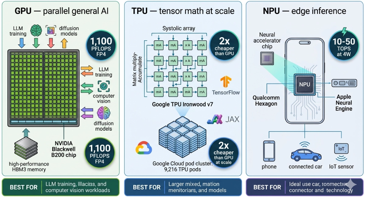
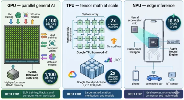
A Graphics Processing Unit (GPU) is a massively parallel processor originally engineered to render pixels for computer graphics but repurposed — and now redesigned — as the default AI accelerator for deep learning training and inference. Modern datacenter GPUs bear little resemblance to their gaming origins: they are purpose-built compute engines optimised for the floating-point matrix operations that power every neural network. NVIDIA’s H100 GPU, built on the Hopper architecture, packs 16,896 CUDA cores, 80GB of HBM3 memory, 3,350 GB/s of memory bandwidth, and delivers up to 3,958 TOPS of INT8 performance. The successor Blackwell B200 pushes this to 288GB of HBM3e and 1,100 petaFLOPS of FP4 inference performance. What makes GPUs uniquely powerful for AI is their combination of raw parallelism, programmability, and the CUDA software ecosystem — 20+ years of libraries, 4 million+ developers, and every major framework (PyTorch, TensorFlow, JAX) optimised for CUDA first. NVIDIA’s H100 costs approximately $3,320 to manufacture and sells for $28,000, with 88.1% gross margins that reflect the genuine moat of the full-stack CUDA platform rather than just the hardware.
Strengths and Advantages
- Universal framework support: PyTorch, TensorFlow, JAX, ONNX, and every major ML library optimises for CUDA first — the path of least resistance for virtually every AI workload
- Training flexibility: Handles any model architecture — transformers, CNNs, diffusion models, GNNs, reinforcement learning — without needing to redesign for specific hardware constraints
- High memory capacity: H100 offers 80GB HBM3; B200 pushes to 192GB; AMD MI350X reaches 288GB — enabling large model training and inference without model partitioning
- Mature ecosystem: CUDA has 20+ years of optimised libraries (cuDNN, cuBLAS, TensorRT), profiling tools, debugging support, and community knowledge that no competitor matches
- Cloud availability: Every major cloud provider — AWS, Azure, GCP, CoreWeave, Lambda Labs — offers GPU instances; pricing pressure from competition is real and growing
- Inference versatility: Handles both real-time low-latency inference and high-throughput batch inference — the same hardware serves training clusters and production serving fleets
Limitations and Constraints
- Power consumption: NVIDIA H100 draws up to 700W per unit — a single 8-GPU DGX H100 system requires ~6.4kW of power plus cooling; datacenter energy costs compound rapidly at scale
- Cost: H100 at $28,000 per unit; B200 at $40,000+ — building even a modest training cluster requires millions in hardware capital before the first model trains
- Supply scarcity: NVIDIA GPU supply has been constrained by TSMC CoWoS packaging capacity — enterprise customers face long lead times and allocation limits
- Cost-efficiency ceiling: GPUs are general-purpose by design — for specialised workloads like large-scale matrix training or on-device inference, purpose-built chips deliver better performance per watt per dollar
- CUDA lock-in: The same ecosystem strength that makes GPUs the safe default also creates switching costs — models optimised for CUDA require significant effort to port to ROCm or other platforms
- Not suited for edge: 700W GPUs cannot run in smartphones, laptops, or battery-powered devices — edge AI inference requires NPUs or mobile SoC solutions
GPU Key Technical Parameters (NVIDIA H100/B200, 2026):
CUDA Cores: 16,896 (H100) — thousands of parallel cores executing floating-point and integer operations simultaneously. Memory: 80GB HBM3 (H100) / 192GB HBM3e (B200) / 288GB HBM3e (AMD MI350X). Memory Bandwidth: 3,350 GB/s (H100) — critical for feeding large model weights to compute units. Furthermore, Performance: 3,958 TOPS INT8 (H100); 1,100 PFLOPS FP4 (B200 Blackwell). Power: 700W TDP (H100); 1,000W (B200). Price: ~$28,000/unit (H100); $40,000+ (B200). Additionally, Software: CUDA ecosystem — PyTorch, TensorFlow, JAX, cuDNN, cuBLAS, TensorRT. Moreover, Interconnect: NVLink/NVSwitch for multi-GPU; InfiniBand for cluster-scale distributed training.
GPU vs TPU vs NPU for AI Workloads: The TPU
Definition
A Tensor Processing Unit (TPU) is a custom application-specific integrated circuit (ASIC) engineered by Google specifically for the matrix multiplication and tensor operations at the core of machine learning workloads. First deployed internally at Google in 2015 and now in its seventh generation with Ironwood (released November 2025), TPUs are built around a systolic array architecture — a grid of multiply-accumulate units where data flows through in a wave pattern, eliminating the memory bottlenecks that limit GPU performance on certain ML workloads. Google’s TPU v1 demonstrated 83 times better performance-per-watt than contemporary CPUs and 29 times better than GPUs for inference workloads. At scale, TPUs cost approximately 2x less than equivalent GPU compute on Google Cloud and large organisations have reported 50% cost reductions when switching matched workloads from GPU to TPU. TPUs scale to pods of up to 9,216 chips connected by Google’s proprietary high-bandwidth interconnect — enabling training runs that would require prohibitively complex multi-GPU cluster engineering to achieve equivalent scale. The key constraint: TPUs are only available through Google Cloud, work best with TensorFlow and JAX (PyTorch support has improved but remains secondary), and are not accessible outside Google’s cloud ecosystem.
Strengths and Advantages
- Cost efficiency at scale: 2x cheaper than GPU compute at scale for matched workloads — large organisations have reported 50% cost reductions on training runs that suit the TPU’s systolic architecture
- Massive pod scaling: Up to 9,216 TPUs per pod connected by Google’s high-bandwidth interconnect — enabling training at a scale that requires far less engineering effort than equivalent multi-GPU cluster setup
- Energy efficiency: 83x better performance-per-watt than CPUs for inference; significantly more efficient than GPUs for large-batch ML workloads at datacenter scale
- Google ecosystem integration: Native integration with Google Cloud AI services, Vertex AI, BigQuery ML, TensorFlow Extended (TFX), and JAX — teams already on Google Cloud get the deepest workflow integration
- Proven at the largest scale: Google uses TPUs to power Search, Photos, Google Translate, and its largest language models — the most battle-tested ML infrastructure at extreme scale
- Continuous generational improvement: Ironwood (v7) delivers substantial throughput gains and energy efficiency improvements over v5/v6 — Google invests in annual TPU generations aligned with its LLM scaling requirements
Limitations and Constraints
- Google Cloud lock-in: TPUs are exclusively available through Google Cloud — organisations that need multi-cloud flexibility, on-premises deployment, or cloud-agnostic infrastructure cannot use TPUs
- Framework dependency: Optimised for TensorFlow and JAX; PyTorch support has improved significantly but is still secondary — teams heavily invested in PyTorch workflows face friction transitioning to TPUs
- Workload specificity: TPUs excel at workloads that fit their systolic array architecture — large batch matrix operations. For irregular compute patterns, dynamic shapes, or highly custom operators, GPUs often outperform TPUs despite the higher cost
- Limited availability for smaller teams: TPU quotas on Google Cloud can be restrictive; access to the largest TPU pods requires enterprise contracts and significant cloud spend commitments
- Debugging complexity: Debugging and profiling TPU workloads is more complex than GPU equivalents — fewer tools, smaller community, and less mature observability compared to the CUDA ecosystem
- Not a general-purpose compute option: Unlike GPUs that serve graphics, gaming, scientific computing, and AI, TPUs are exclusively ML accelerators — no alternative use cases if AI workloads change
TPU Key Technical Parameters (Google TPU Ironwood v7, 2026):
Architecture: Systolic array — matrix multiply-accumulate units arranged in a grid through which data flows sequentially, eliminating memory bandwidth bottlenecks for large-batch ML. Scale: Up to 9,216 TPUs per pod; available as individual chips, slices, and full pods via Google Cloud. Performance: Varies by generation; Ironwood delivers substantial improvements in throughput and energy efficiency over v5p. Furthermore, Memory: HBM2e per chip; total pod memory scales to petabytes of aggregate capacity. Availability: Google Cloud only — Cloud TPU service; Vertex AI integration; not available on-premises or other clouds. Additionally, Frameworks: TensorFlow, JAX (native); PyTorch via XLA bridge (improved in 2025–2026). Moreover, Cost: ~2x cheaper than equivalent GPU at scale for matched workloads; hourly rental on Google Cloud varies by pod size and generation.
GPU vs TPU vs NPU for AI Workloads: The NPU
Definition
A Neural Processing Unit (NPU) is a highly specialised, ultra-low-power AI accelerator designed specifically for running trained neural networks on edge devices — smartphones, laptops, tablets, autonomous vehicles, IoT sensors, and industrial equipment — where cloud connectivity is unavailable, latency requirements are measured in milliseconds, power budgets are measured in watts rather than kilowatts, and user privacy demands that data stay on the device. Unlike GPUs (designed for flexibility across workloads) and TPUs (designed for large-scale cloud training), NPUs are optimised for a single task: inference — running an already-trained model against new input data as fast and as efficiently as possible. NPUs achieve 40–60 times better energy efficiency than GPUs for edge inference workloads by abandoning general-purpose programmability entirely in favour of fixed-function neural network execution circuits. Apple’s Neural Engine in the M4 chip delivers 38 TOPS within a total chip TDP of approximately 25 watts. Qualcomm’s Hexagon NPU inside the Snapdragon X Elite delivers 45 TOPS. Intel’s integrated NPU in Core Ultra processors delivers 13 TOPS. Over 970 million smartphones shipped with NPUs in 2025 — making the NPU, by sheer unit volume, the most widely deployed AI chip on the planet, even though most users have never heard the term.
Strengths and Advantages
- Extreme energy efficiency: 40–60x more power-efficient than GPUs for edge inference — enables AI features on smartphones, wearables, and IoT sensors that simply cannot connect to a GPU cluster
- Zero cloud cost for inference: Once a model is deployed to device, inference is free — no API charges, no cloud egress fees, no per-query costs that compound at billions of inferences per day across a user base
- Privacy-first inference: Data processed on-device never leaves the user’s hardware — face recognition, health monitoring, voice processing, and biometric authentication stay local
- Ultra-low latency: Eliminates the round-trip to a cloud server — on-device NPU inference can respond in under 10ms vs 100–500ms for cloud inference including network round-trip
- Always-available: Works without internet connectivity — critical for automotive AI, industrial systems, healthcare devices, and rural deployments where reliable cloud access cannot be assumed
- Embedded at zero marginal cost: NPUs are integrated into SoCs (System on Chips) that customers already buy for other reasons — the AI acceleration is included in the chip price, not a separate hardware investment
Limitations and Constraints
- Inference-only: NPUs cannot train models — training requires cloud GPU or TPU resources; NPUs only run pre-trained, optimised models compressed to fit within tight memory and compute budgets
- Model size constraints: Current flagship NPUs handle models up to approximately 1–7 billion parameters on-device — GPT-4 class (100B+ parameter) models cannot run on NPUs as of 2026
- Model optimisation required: Models must be quantised (typically to INT8 or INT4), pruned, and compiled for the target NPU using vendor-specific toolchains (Apple Core ML, Qualcomm SNPE, Intel OpenVINO) — converting a GPU-trained model to NPU takes significant engineering effort
- Vendor fragmentation: Apple Neural Engine, Qualcomm Hexagon, MediaTek APU, Samsung Exynos NPU, Intel AI Boost, and Arm Ethos all have different instruction sets, toolchains, and performance characteristics — cross-device deployment requires separate optimisation for each platform
- Not suitable for training or complex reasoning: NPUs lack the memory capacity, floating-point precision, and programmability needed for model training, fine-tuning, or running complex multi-step reasoning chains
- Limited software ecosystem: Compared to GPU’s CUDA maturity, NPU toolchains vary significantly in quality and developer experience — especially for non-Apple, non-Qualcomm platforms
NPU Key Technical Parameters (2026 Flagship Devices):
Apple M4 Neural Engine: 38 TOPS; integrated in Apple Silicon — Macs, iPads, iPhones; Core ML toolchain. Qualcomm Hexagon NPU (Snapdragon X Elite): 45 TOPS; 45% power reduction for voice processing; Snapdragon Neural Processing Engine (SNPE) toolchain. Intel AI Boost (Core Ultra): 13 TOPS; integrated in AI PC processors; OpenVINO toolchain. Furthermore, High-Performance NPUs: 15–50+ TOPS for premium smartphones, edge AI servers, smart robots, automotive systems. Power: 4–10W typical (vs GPU’s 700W) — 40–60x more efficient for inference. Additionally, Model Support: Efficiently runs models up to 1–7B parameters; handles MobileNet, EfficientNet, BERT-Tiny, custom vision/NLP models. Moreover, Deployment: Frameworks include Apple Core ML, Qualcomm SNPE, Intel OpenVINO, ONNX Runtime, TensorFlow Lite, MediaPipe.
GPU vs TPU vs NPU for AI Workloads: Architecture Deep Dive
How Each Architecture Approaches Matrix Multiplication
Matrix multiplication is the fundamental operation of every neural network — it is what happens billions of times per second when a model processes input data. GPU vs TPU vs NPU differ most fundamentally in how their silicon implements this operation:
GPU Approach
Flexible parallel cores: Thousands of CUDA cores operate independently, each capable of executing any floating-point instruction. The GPU schedules matrix operations across these cores dynamically.
- Tensor Cores (H100: 528 Tensor Cores) accelerate mixed-precision matrix ops specifically
- VRAM stores model weights; high-bandwidth memory (HBM3: 3,350 GB/s) feeds cores continuously
- Flexibility means any model architecture works, but also means energy is spent on general programmability overhead
- NVLink interconnect enables multi-GPU scaling for models too large for single-GPU memory
TPU Approach
Systolic array: A 2D grid of simple multiply-accumulate units. Data flows through in a wave — each unit receives data from its neighbour, computes, and passes results downstream. No random memory access.
- Eliminates the memory bandwidth bottleneck that limits GPU performance on regular large-batch matrix operations
- Extremely efficient for the specific matrix math of transformer and CNN forward/backward passes
- Deterministic execution — same input always takes the same time; enables precise performance modelling
- Pod interconnect allows massive-scale distributed computation with minimal engineering overhead
NPU Approach
Fixed-function neural network engines: Dedicated hardware circuits for convolution, pooling, attention, and activation functions. No general-purpose cores — only the operations neural networks actually use.
- Quantised operations (INT8, INT4) match the reduced precision acceptable for inference, saving further energy
- On-chip SRAM stores frequently accessed weights, avoiding external memory access latency and power cost
- Parallel sub-engines handle different network layers simultaneously — pipeline execution across the network
- Deep SoC integration shares power management, memory controllers, and thermal budget with the rest of the device
GPU vs TPU vs NPU for AI Workloads: Performance Metrics Comparison
| Metric | GPU (NVIDIA H100) | TPU (Google Ironwood v7) | NPU (Qualcomm Hexagon / Apple M4) |
|---|---|---|---|
| Peak AI Performance | 3,958 TOPS (INT8); 989 TFLOPS (FP16) | Several hundred to thousands of TOPS (varies by config) | 38–45 TOPS (flagship mobile); 10–50 TOPS range |
| Memory | 80GB HBM3 (H100); 288GB HBM3e (B200) | HBM2e per chip; scales with pod size | Shares system LPDDR5 — typically 8–32GB total |
| Memory Bandwidth | 3,350 GB/s (H100) | High via systolic array design; no random DRAM access | ~68–100 GB/s (LPDDR5); limited by shared system memory |
| Power Consumption | 700W TDP (H100); 1,000W (B200) | Varies; higher than NPU but better perf/watt at scale | 4–10W typical; 40–60x more efficient than GPU for inference |
| Performance/Watt | Baseline for comparison | ~29x better than GPU (TPU v1 vs GPU for inference) | 40–60x better than GPU for edge inference workloads |
| Inference Latency | Low (datacenter) — sub-millisecond batch; 100–300ms per-request with network | Optimised for throughput over per-request latency | Under 10ms on-device — no network round-trip |
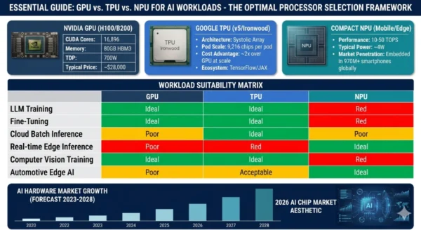
12 Critical Differences: GPU vs TPU vs NPU for AI Workloads
The GPU vs TPU vs NPU for AI workloads comparison below covers every key dimension — from architecture and use case to cost, availability, ecosystem, and power profile — giving you the complete picture for workload matching in 2026.
Aspect | GPU | TPU | NPU |
|---|---|---|---|
| Primary Design Purpose | General parallel computation — originally graphics, repurposed and redesigned for AI training and inference | Large-scale ML training and inference — purpose-built for tensor/matrix operations from day one | On-device edge AI inference — ultra-low power neural network execution in smartphones, laptops, IoT |
| Architecture | Thousands of flexible CUDA/Tensor cores with large VRAM and high-bandwidth memory | Systolic array of matrix multiply-accumulate units — data flows through in a wave pattern | Fixed-function neural network engines — dedicated circuits for convolution, attention, activation |
| Best Workload | Model training (all types), fine-tuning, general inference, computer vision, LLMs | Large-scale training on Google Cloud, high-throughput batch inference, TensorFlow/JAX workloads | Real-time on-device inference — voice, vision, NLP on smartphones, laptops, automotive |
| Power Consumption | 700W–1,000W per unit (datacenter GPU) — requires significant infrastructure cooling | Higher than NPU but significantly better perf/watt than GPU for matched batch workloads at scale | 4–10W typical — 40–60x more efficient than GPU for inference; battery-compatible |
| Cost Model | $28,000–40,000/unit; or $2–8/hour on cloud — flexible pricing but significant capital or operational cost | Cloud rental only on Google Cloud; ~2x cheaper than GPU at scale for matched workloads | Embedded in device SoC — zero incremental hardware cost once device is purchased |
| Availability | Multiple cloud providers (AWS, Azure, GCP, CoreWeave) + on-premises purchase; broadest availability | Google Cloud only — no on-premises, no AWS, no Azure; hard dependency on Google’s platform | Embedded in devices — available in 970M+ smartphones globally; no cloud access needed |
| Training Support | Full training capability — the dominant choice for training all model sizes from prototype to frontier scale | Full training capability — optimised for large-scale training at Google Cloud pod scale | Inference only — no model training capability; NPUs run pre-trained, compressed models |
| Framework Support | PyTorch, TensorFlow, JAX, ONNX, all major frameworks — CUDA is the universal target | TensorFlow, JAX (native); PyTorch via XLA bridge (improving); not all frameworks fully supported | Vendor-specific toolchains: Core ML (Apple), SNPE (Qualcomm), OpenVINO (Intel), TFLite, ONNX RT |
| Privacy Profile | Data sent to cloud for processing — applicable data regulations and privacy policies apply | Data sent to Google Cloud — Google’s data handling policies apply; not suitable for some regulated workloads | Data stays on device — ideal for sensitive applications: health, biometrics, personal communications |
| Latency Characteristics | Low for datacenter serving; 100–500ms total for cloud inference including network round-trip | Optimised for throughput over per-request latency — best for batch processing, not interactive real-time | Under 10ms on-device — eliminates network round-trip entirely; near-instant local response |
| Market Position | NVIDIA controls ~87% of market; AMD MI-series is primary challenger; $51.2B quarterly revenue FY2026 | Google’s internal and cloud product; competitors include AWS Trainium, Microsoft Maia, Meta MTIA | Qualcomm Hexagon, Apple Neural Engine, Intel AI Boost, MediaTek APU, Samsung Exynos NPU |
| Future Direction | Annual architecture cadence (Blackwell → Rubin 2026); growing competition from custom ASICs | Custom ASIC shipments growing 44.6% in 2026; Anthropic ordered 1M TPUs from Google | On-device LLM inference expanding (1–7B params in 2026); Qualcomm AI200 entering data center in 2026 |
GPU vs TPU vs NPU for AI Workloads: Use Cases and Workload Matching
GPU — Ideal Workloads
- LLM training: Training GPT, Llama, Mistral, and custom transformers from scratch — the H100 cluster is the universal standard for frontier model training
- Fine-tuning: Adapting pre-trained models to specific domains (medical, legal, code) — requires GPU memory capacity and training framework support
- Diffusion model training: Stable Diffusion, DALL-E, Sora-class video generation — highly memory-intensive workloads matching GPU HBM capacity
- Research and prototyping: Experimenting with new architectures, hyperparameter tuning, and iteration — GPU flexibility handles any model design
- Real-time inference at scale: Serving LLM API responses (ChatGPT, Claude, Gemini) at millions of queries per hour — GPU clusters with tensor parallelism
- Computer vision at datacenter scale: Training and serving detection, segmentation, and classification models for enterprise applications
TPU — Ideal Workloads
- Large-scale training on Google Cloud: Teams already in Google’s ecosystem training transformer models at pod scale — where the 2x cost advantage over GPU is most valuable
- High-throughput batch inference: Processing millions of documents, images, or queries overnight where latency per request is less important than total cost and throughput
- TensorFlow and JAX workflows: Organisations that have built their ML infrastructure on TensorFlow or JAX and want the hardware most tightly integrated with those frameworks
- Google AI services consumers: Companies leveraging Vertex AI, BigQuery ML, or Google AI APIs where TPUs power the underlying inference and training infrastructure
- Research at frontier scale: Academic and enterprise research requiring access to hundreds or thousands of accelerators simultaneously — TPU pods provide this more accessibly than equivalent GPU cluster setup
NPU — Ideal Workloads
- On-device voice and speech: Wake word detection, real-time transcription, language translation, voice assistant processing — all running locally with no cloud dependency
- On-device computer vision: Face recognition for biometric authentication, object detection in camera apps, augmented reality scene understanding, document scanning
- Privacy-critical AI: Health monitoring (heart rate analysis, ECG interpretation), biometric authentication, personal financial analysis — data that legally or ethically must stay on device
- Automotive AI: ADAS (advanced driver assistance), cabin monitoring, occupant detection — latency requirements too tight for cloud round-trips and connectivity too unreliable
- Industrial IoT: Predictive maintenance sensors, quality control cameras on production lines, agricultural monitoring systems — environments without reliable cloud connectivity
- Small on-device LLMs: 1–7 billion parameter models running locally (Phi-3 Mini, Mistral 7B quantised) — increasingly practical on 2026 flagship NPUs
GPU vs TPU vs NPU for AI Workloads: Industry Application Matrix
| Industry / Application | GPU Role | TPU Role | NPU Role |
|---|---|---|---|
| LLM / Generative AI | Primary — training and cloud inference serving | Alternative at scale — Google-ecosystem training | Emerging — on-device small model inference |
| Healthcare AI | Medical imaging model training, drug discovery | Large-scale genomics processing on Google Cloud | Wearable health monitoring, ECG analysis on device |
| Autonomous Vehicles | Perception model training in datacenter | Fleet-scale data processing and retraining | Real-time driving inference in the vehicle |
| Smartphones | No role (too power-hungry for mobile) | No role (cloud-only, no mobile deployment) | Primary — all on-device AI features |
| Enterprise Search / RAG | Embedding generation, retrieval model training | Large-scale document processing on GCP | On-device document search and summarisation |
| Industrial IoT | Central AI server training and data processing | Cloud-scale anomaly detection model training | Real-time edge inference on factory floor sensors |
GPU vs TPU vs NPU for AI Workloads: Cost, Performance and Market Analysis
NVIDIA GPU Revenue
$51.2B
Single quarter data centre revenue Q3 FY2026 — +66% YoY; 90% of total company revenue
AI Hardware Market
$65.35B
Global AI hardware market 2026 — growing to $296.3B by 2034 at 18% CAGR
NPU Devices
970M+
Smartphones with NPUs shipped globally in 2025 — the most widely deployed AI chip by volume
Custom ASIC Growth
44.6%
Custom ASIC (incl. TPU) shipment growth in 2026 vs 16.1% for GPU — hyperscalers building own chips
GPU Cost Economics (2026)
| GPU | Unit Price | Cloud Rental | Power (TDP) | Annual Electricity Cost* |
|---|---|---|---|---|
| NVIDIA H100 (Hopper) | ~$28,000 | $2–4/hour (A100/H100 class) | 700W | ~$613/year at $0.10/kWh |
| NVIDIA B200 (Blackwell) | ~$40,000+ | $4–8/hour (B200 class) | 1,000W | ~$876/year at $0.10/kWh |
| AMD MI350X | $25,000–35,000 est. | Varies by cloud provider | 750W est. | ~$657/year at $0.10/kWh |
| 8-GPU Training Server (H100) | $200,000–400,000 | $16–32/hour (8-GPU instance) | ~6.4kW | ~$5,600/year per server |
*Electricity cost calculated at $0.10/kWh, 24/7 operation. Actual datacenter costs include cooling overhead (PUE factor ~1.3–1.6), typically adding 30–60% to the base electricity figure.
The Economics of Scale: When TPU Beats GPU
| Workload Scale | GPU Economics | TPU Economics | Verdict |
|---|---|---|---|
| Small experiments (1–10 GPU-days) | Flexible cloud GPU spot instances; on-demand pricing | TPU setup overhead not justified; less tooling flexibility | GPU wins — flexibility and framework support matter more than per-unit cost |
| Medium training runs (10–1,000 GPU-days) | Reserved GPU instances; 1–3 year commitments for discount | TPU competitive; cost advantage emerging for TF/JAX workloads | Depends on ecosystem — GPU if PyTorch-first; TPU competitive for TF/JAX |
| Large-scale training (1,000+ GPU-days) | High cost; complex multi-GPU cluster management | ~2x cheaper; pod scaling significantly simpler; 50% cost reduction reported | TPU wins for Google Cloud teams — meaningful cost and operational advantage |
| High-volume batch inference | Serving cluster at $2–8/hour; autoscaling GPU fleets | TPU inference cost advantage for large batches; better throughput per dollar | TPU competitive for batch; GPU for real-time and mixed workloads |
The Inference Market Split: Training vs Inference Economics in 2026
The Inference Tipping Point
AI inference demand is projected to exceed training demand by 2026, fundamentally reshaping the AI chip market. Training is a one-time (or periodic) investment. Inference creates continuous, compounding operational costs as user bases grow. A model trained once may serve billions of inferences over its lifetime — and the economics of each inference, multiplied at scale, dwarf the one-time training cost. This is why GPUs, TPUs, and NPUs are all competing most aggressively for inference workloads in 2026: edge inference on NPUs eliminates cloud costs entirely; TPUs offer 2x lower cost for cloud batch inference; and specialised inference-focused ASICs (AWS Inferentia, Groq LPU, Positron Atlas) are emerging to compete with general-purpose GPUs for the inference dollar.
GPU vs TPU vs NPU for AI Workloads: Decision Framework
Matching Hardware to Workload
The GPU vs TPU vs NPU for AI workloads decision is fundamentally a workload-matching exercise, not a brand preference. Start with three questions: What stage of the AI lifecycle am I in — training, fine-tuning, or inference? Where does execution need to happen — cloud datacenter, cloud edge, or physical device? What is my primary constraint — maximum performance, minimum cost per inference, minimum power, or maximum privacy? The answers to these three questions will determine the right chip family for your workload in approximately 80% of real-world cases.
Choose GPU When:
- You are training or fine-tuning any model and need framework flexibility — GPU + CUDA is the universal starting point
- Your team uses PyTorch as its primary framework and is not invested in TensorFlow or JAX
- You need multi-cloud flexibility — run on AWS today, Azure tomorrow, on-premises next quarter
- You are running diverse workloads including computer vision, NLP, and generative models that benefit from one flexible hardware platform
- You need real-time, low-latency inference at cloud scale — GPU serving clusters optimised for interactive use
- You are a startup or research team at early stage — GPU provides the fastest path from prototype to production regardless of final infrastructure target
Choose TPU When:
- You are already committed to Google Cloud and use TensorFlow or JAX as your primary framework — the ecosystem integration advantage is real
- You are running large-scale training jobs (1,000+ GPU-day equivalents) where the 2x cost advantage translates to significant dollar savings
- Your workloads are dominated by large-batch matrix operations that fit the systolic array architecture — transformers and CNNs at scale
- You are processing massive datasets for batch inference where throughput matters more than per-request latency
- You want the hardware that Google itself uses to train Gemini and power its AI services — and you are on Google Cloud infrastructure
- Cost reduction from GPU to TPU for matched workloads is your primary budget mandate, and platform lock-in to Google Cloud is an acceptable trade
Choose NPU When:
- You are building features that must work offline — no internet, no cloud, immediate local response regardless of connectivity
- User privacy is non-negotiable — health data, biometrics, personal communications, financial behaviour must not leave the device
- Latency requirements are under 10–50ms — automotive, voice interfaces, AR/VR, and real-time video analysis cannot tolerate cloud round-trips
- You are building a mobile app, smart device, or IoT product where the compute budget is measured in milliwatts, not kilowatts
- Your inference costs at scale are prohibitive — serving 100M users’ on-device AI features for free (no cloud inference cost) vs paying per-query API costs
- Your model has been validated at cloud scale and you are now deploying it to end-user devices — NPU is the inference target for on-device AI product features
GPU vs TPU vs NPU Quick Decision Table
| Situation | Best Choice | Reason |
|---|---|---|
| Training a new LLM from scratch | GPU | Universal framework support, training flexibility, multi-GPU scaling |
| Fine-tuning on Google Cloud with TensorFlow | TPU | 2x cost advantage, native TF integration, pod scaling |
| Building an on-device voice assistant for iOS | NPU (Apple Neural Engine) | On-device privacy, zero latency, zero cloud cost, Core ML toolchain |
| Running a RAG system for 10M API queries/day | GPU | Real-time inference at scale, CUDA-optimised serving frameworks |
| On-device face recognition for smartphone camera | NPU | 40–60x more efficient, stays on device, no connectivity needed |
| Batch processing 1 billion documents monthly on GCP | TPU | Batch throughput, systolic efficiency, 50% cost reduction at scale |
| ADAS real-time inference in a vehicle | NPU (automotive SoC) | Latency critical, connectivity unreliable, always-on, low power |
| Research on new model architectures | GPU | Flexibility to run any architecture without hardware constraint |
| Running Phi-3 Mini locally on a laptop | NPU | Qualcomm/Intel NPU handles 3.8B param models locally at 4–10W |
| Maximum performance, cost not primary concern | GPU (NVIDIA B200) | Highest raw performance; CUDA ecosystem; handles any workload |
Frequently Asked Questions
NPUs are ultra-specialised inference-only chips that sacrifice training capability and model size for extreme energy efficiency — 40–60x more power-efficient than GPUs for edge inference, running on milliwatts inside your phone or laptop. In practice: GPU for training, TPU for Google-ecosystem cloud training and batch inference, NPU for on-device inference.
TPUs, despite their cost and efficiency advantages, are constrained to Google Cloud and work best with TensorFlow/JAX — most of the industry’s ML code is written in PyTorch. NPUs are measured in different units (TOPS for inference) vs GPU market share (which is measured in training and cloud inference) — so the 87% figure and the 970M NPU smartphone number measure fundamentally different markets that do not directly compete.
All model training happens on GPU clusters or TPU pods in the cloud. Once trained and compressed (quantised to INT8 or INT4), a model is compiled for the target NPU using vendor toolchains (Core ML, SNPE, OpenVINO) and deployed to device for inference. The training cloud and the inference edge device are fundamentally different parts of the AI lifecycle and currently require different hardware entirely.
For most teams, this means: start on GPU with CUDA, and only evaluate TPU or custom silicon once you have validated your workload and can afford the engineering effort to port. AMD’s ROCm has narrowed the gap (performance difference with CUDA dropped from 40–50% to 10–30% on many workloads in 2025–2026), but the 10x developer activity gap between CUDA and ROCm remains the decisive practical factor.
Higher floating-point precision delivers better model accuracy but lower raw throughput. PFLOPS (Peta Floating-Point Operations Per Second) is simply TFLOPS at a larger scale — the B200 GPU’s 1,100 PFLOPS FP4 means 1.1 quadrillion four-bit floating-point operations per second. Memory bandwidth (GB/s) measures how fast data can move between memory and compute — often the actual bottleneck for large model inference where weights must constantly be loaded from HBM. The critical insight is that TOPS numbers across different chip types are not directly comparable: 45 TOPS on an NPU at 4W is a fundamentally different capability profile than 3,958 TOPS on an H100 at 700W — same unit, completely different scale, purpose, and power envelope.
OpenAI is building its first custom ASIC with Broadcom and TSMC for mass production in 2026. The trend is structural: custom ASIC shipments are growing 44.6% in 2026 vs 16.1% for GPU shipments. For enterprises that are not hyperscalers, the economics are different — the design cost of a custom AI chip starts at tens of millions of dollars, which is only justified when chip volume is large enough to amortise that cost below NVIDIA’s $28,000 retail price. Until then, GPUs remain the economically rational choice despite the premium.
Performance is approximately 20–40 tokens per second on flagship NPUs for 3–7B models, which is adequate for text completion and summarisation but slower than cloud LLM APIs. Models above 7–13B parameters remain impractical for NPU deployment in 2026 — they require too much memory and produce output too slowly. Qualcomm’s AI200 data centre chip (entering market in 2026) blurs the NPU/GPU boundary by targeting inference at data centre scale with NPU-style efficiency at much larger model sizes.
TPU makes sense for LLM training when: you are already on Google Cloud with a significant existing TensorFlow or JAX investment, you are training at a scale where the 2x cost advantage represents millions of dollars in savings, and you have the engineering capacity to port your training code to work efficiently on XLA. Anthropic’s order of 1 million TPUs from Google signals that the largest frontier AI labs at extreme scale are evaluating the economics of TPU at their specific workload profiles — but for most teams training in the 1B–70B parameter range, GPU remains the pragmatic default.
For cloud inference: GPUs compete with TPUs, specialised inference ASICs, and the next generation of efficient chips optimised specifically for transformer serving. For edge inference: NPUs are dominant and expanding — on-device LLMs become practical for larger model classes as NPU TOPS ratings and device memory expand annually. IBM noted that 2026 is “the year of frontier versus efficient model classes” — a split between massive cloud-resident models and efficient device-resident models that directly maps onto the GPU/TPU vs NPU hardware distinction.
FPGAs offer lower latency than GPUs for specific inference tasks and better flexibility than fixed-function ASICs, but lower raw performance than either — making them most suitable for ultra-low-latency inference applications like algorithmic trading or 5G baseband processing. The hierarchy runs: CPU (most flexible, worst for AI) → GPU (highly parallel, good for AI, flexible) → FPGA (reconfigurable, specific use cases) → TPU/ASIC (purpose-built, excellent for specific workloads, less flexible) → NPU (fixed-function inference, most efficient for on-device AI). In 2026, the market is decisively moving toward more specialised silicon at every layer of the AI stack.
GPU vs TPU vs NPU for AI Workloads: Final Takeaways for 2026
The GPU vs TPU vs NPU for AI workloads question does not have a single correct answer — it has three correct answers that apply at different layers of the AI stack. Every serious AI system in 2026 actually uses all three: GPUs or TPUs to train and fine-tune models in the cloud, and NPUs to run those models on end-user devices. The key is matching the right chip to the right stage of the AI lifecycle.
GPU — Key Takeaways:
- NVIDIA controls 87% market; $51.2B quarterly revenue FY2026
- H100: 16,896 CUDA cores, 80GB HBM3, 700W, $28,000
- Universal framework support: PyTorch, TF, JAX, all ML libs
- Training, fine-tuning, and general inference — the safe default
- CUDA ecosystem moat: 20+ years, 4M+ developers
- Custom ASIC competition growing 44.6%/year, GPU 16.1%
TPU — Key Takeaways:
- Google’s custom ASIC; now in 7th generation (Ironwood, Nov 2025)
- Systolic array: 83x better perf/watt than CPU; 29x better than GPU
- 2x cheaper than GPU at scale; 50% cost reduction reported
- Up to 9,216 TPUs per pod — massive scale training
- Google Cloud only; TF/JAX native; PyTorch improving
- Anthropic ordered 1M TPUs — signals frontier lab adoption
NPU — Key Takeaways:
- 970M+ smartphones shipped with NPUs in 2025 globally
- 40–60x more efficient than GPU for edge inference
- 4–10W power vs 700W per datacenter GPU
- Zero cloud cost, zero latency, zero connectivity needed
- Apple Neural Engine 38 TOPS; Qualcomm Hexagon 45 TOPS
- 2026: runs 1–7B parameter models on-device
Practical Recommendation for 2026:
Start with GPU for any new AI project that involves training — the CUDA ecosystem, PyTorch integration, and multi-cloud availability make it the lowest-risk starting point regardless of long-term infrastructure plans. Evaluate TPU when you are on Google Cloud, your workloads run at scale (1,000+ GPU-day equivalents), and the 2x cost advantage outweighs the framework and ecosystem migration effort. Deploy to NPU when your trained model needs to run on user devices — optimise, quantise, and compile your model for the target NPU once you have validated its performance in the cloud. In the GPU vs TPU vs NPU for AI workloads comparison, the best-performing AI systems of 2026 do not choose one — they run all three at different layers of their architecture.
Related Topics Worth Exploring
MLOps vs DevOps
GPU clusters, TPU pods, and on-device NPU deployments all require different operational approaches. Understand how MLOps platforms handle model training pipelines on GPU infrastructure, manage model registries across hardware targets, and monitor model drift in NPU-deployed edge systems — the operational layer above the AI hardware.
Claude Code vs GitHub Copilot
The AI coding tools generating code in 2026 run on the same GPU infrastructure you are evaluating. Claude Code’s capabilities are powered by Anthropic’s GPU and TPU clusters. Understanding the hardware that runs foundation models gives you insight into the economics and scaling constraints of the AI tools transforming software development.
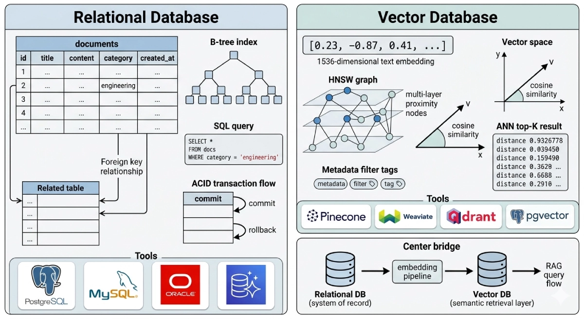
Vector Database vs Relational Database
GPU inference endpoints generate vector embeddings that need to be stored and searched at low latency. The choice of vector database directly affects the GPU compute requirements for your AI inference architecture — understanding both the chip layer and the data layer is essential for designing efficient AI systems in 2026.